Celestron EdgeHD Back Focus Tolerance
Celestron Edge-HD technology
The Celestron EdgeHD (EHD) is an advanced, flat-field, aplanatic series of telescopes designed for visual observation and imaging with astronomical CCD cameras and full-frame digital SLR cameras.
The EHD technology is based to the traditional Schmidt-Cassegrain telescope (SCT) layout associated with a corrector inside the main mirror central baffle. This configuration delivers a flat and coma free field up to 42mm in diameter, consistent with full frame chips (24m x 36mm).
Celestron EHD Optical Layout
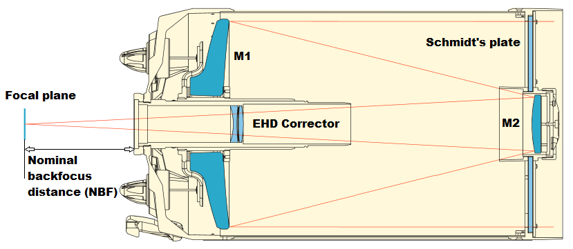
A EHD scope achieves its full capability when the focal plane is placed at a nominal back focus distance (NBF) from the scope visual back.
Here are the Celestron recommended distances for various EHD models behind the surface of the telescope’s rear cell 2″ (for C8) and 3″ (for C9.25, C11, C14) threaded baffle tube lock nut:
- C8 133.35 mm
- C9.25 146.05 mm
- C11 146.05 mm
- C14 146.05 mm
This is the distance where the imaging camera sensor should be located. It should be understood here that by moving the primary mirror (M1) its is possible to reach focus at a different distance than the NBF, in fact SCTs allow for a very large infocus range, many inches in size.
However when the actual focus distance is different than the NBF there is a progressive drop in performance.
The goal here is to discuss the nature and implication of it and define a practical tolerance for the NBF.
Here the data, associated calculations and plots are based on a C11 EHD, the conclusions are also relevant for C14, and in some degrees to C9.25.
Here is a link to a Celestron support article discussing the same topic.
Considerations on EHD Back Focus Tolerance under Seeing Limited Conditions
Here back on Earth we are seldom diffraction limited. While a C11 scope at f/10 can deliver a 0.4″ (arc-second) Airy disc FWHM (or about 13 microns spot diameter for ~80% of encircled energy) in the visible (550nm), the inevitable atmospheric turbulence, or seeing, is usually much more than this.
Below the typical seeing we should expect to experience:
- Excellent ~0.5″ (Exceptional locations only)
- Good ~1″ (Good locations, few good nights)
- Average ~2″ (Most of the locations, most of the nights)
- Bad/Poor >3″ (Not a good night for astrophotography)
In order to set a realistic and practical value to the NBF tolerance we should consider the impact of being offset from the NBF relative to the seeing condition.
The plot below (made from public available Celestron’s data) sketches for a C11 EdgeHD the diameter of the the spot (from a star) for ~80% of the encircled energy under a diffraction limited condition (no seeing) function of the offset value from the NBF (all in meter). It provides two off axis curves (in blue), one at 13.5mm for APS-C chips (DSLR) and one at 21mm for full frame chips (24×36 mm format). The read line shows the diffraction limit.
Fig. 1: C11 EHD Spot diameter versus offset from nominal backfocus (NBF) offset
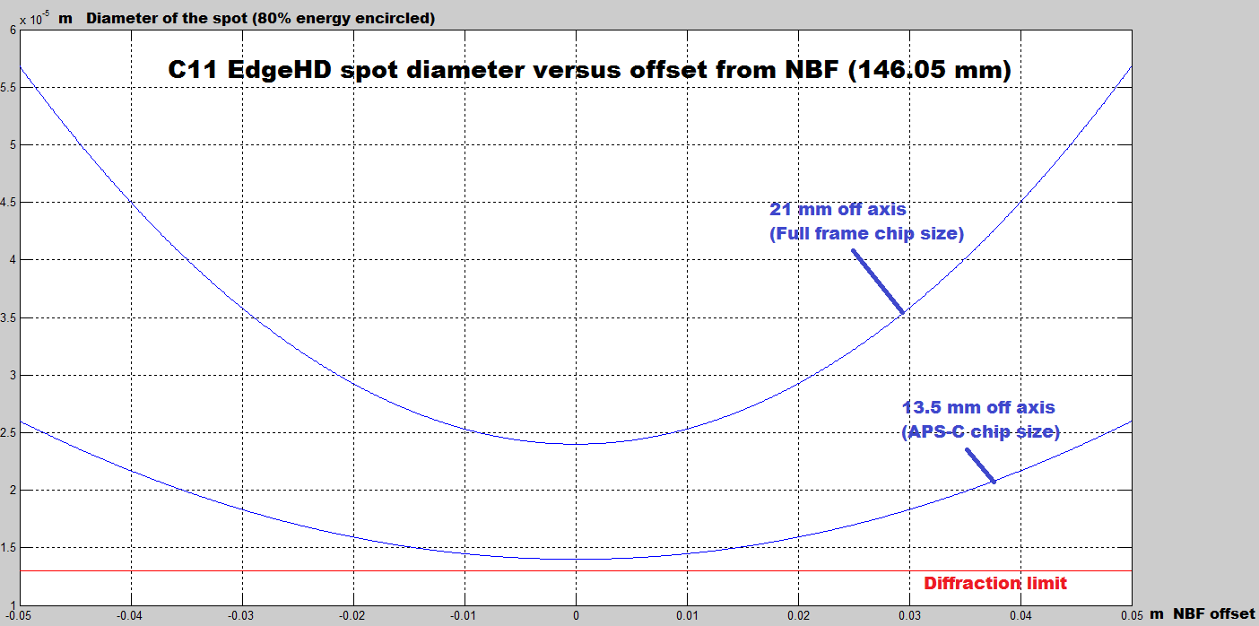
We see that at the NBF distance (offset = 0) the scope is essentially diffraction limited up to 13.5mm off axis, at 21mm off axis the spot size is close to twice the diffraction limit (red line). This is a very impressive performance.
We also see that for APS-C chips (13.5mm off axis, or 27mm in diagonal) we also reach twice the diffraction limit spot diameter for an offset around +/-50 mm (2″) from the NBF.
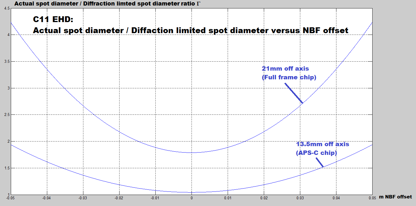
The next plot summarizes this using the ratio Γ between the actual spot diameter and its diffraction limited diameter (13 microns at f/10).
Fig. 2: C11 EHD Actual/diffracted spot diameter ratio v.s. nominal backfocus offset
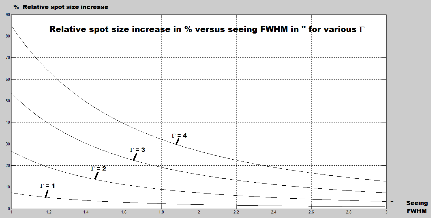
For convenience from now on we’ll use the ratio Γ in our calculations and plots. There is no correlation between the spot diameter sets by the diffraction limit, as well as the scope optics, and the seeing, which is random in nature. The subsequent calculations use this property and assume long exposures (one minute or more) under a seeing larger than the diffraction/optics limit.
Fig. 3: Actual spot FWHM verus seeing FWHM
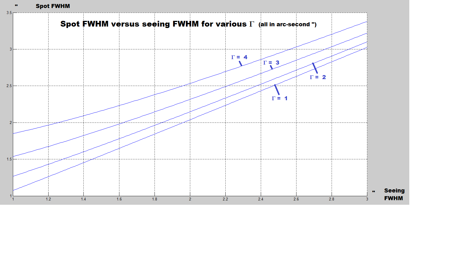
The above plot shows the actual spot FWHM versus the seeing FWHM for various Γ. The former is always larger than the latter, since the diffraction will at least (Γ=1) adds its contribution to the seeing. However for Γ=1 both values are quite close.
The plot below shows the same thing but relative to a spot diameter which would be seeing limited only (perfect optics, no diffraction).
The increase in spot size is given in %, one more time one can see that for Γ=1 (the diffraction limit case) the change in spot size if very little, less than 10% for a 1″ seeing (for a C11 at f/10).
We will consider here that less than 10% difference is negligible and below the human perception, at the level of the noise floor (here we are still assuming that everything else is perfect, including tracking).
Fig. 4: Relative spot size increase v.s. seeing FWHM
Assuming we limit the maximum spot size increase at 10%, let’s analysis the consequences on the NBF tolerance (offset from NBF) for 1″ (good) and 2″ seeing FWHM (average), as well as for APS-C and full frame chips.
- 1″ seeing
The plot of fig. 4 above suggests that we would meet our 10% limit around Γ=1.2 (the exact number being Γ=1.187).
For APS-C chips (13.5mm off axis) the plot in fig. 2 tells us that we reach Γ=1.2 for an offset of +/-20mm, near one inch.
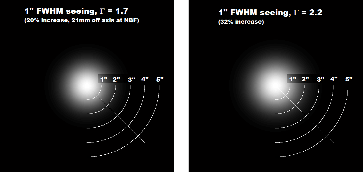
For a full frame chips (21mm off axis) the 10% limit is exceeded even at the NBF distance (offset=0), for which Γ is already 1.7, leading to about 20% increase in spot diameter on the sensor corners. We are starting to face the off axis limits of the optical system.
Therefore we would consider a 10% increase relative to this 21mm off axis spot diameter (at NBF) instead of the diffraction limit (our baseline is now the scope optical off axis limit). This results to a total of 32% (1.2 x 1.1 = 1.32). Under this condition we reach 32% at Γ=2.2, leading to +/-22 mm of offset. - 2″ seeing
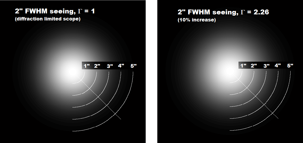
The 10% limit is reached for Γ=2.26.
For APS-C chips this leads to an offset of more than +/-50mm (or about two inches).
While full frame chips offset is about +/-25mm, or one inch.
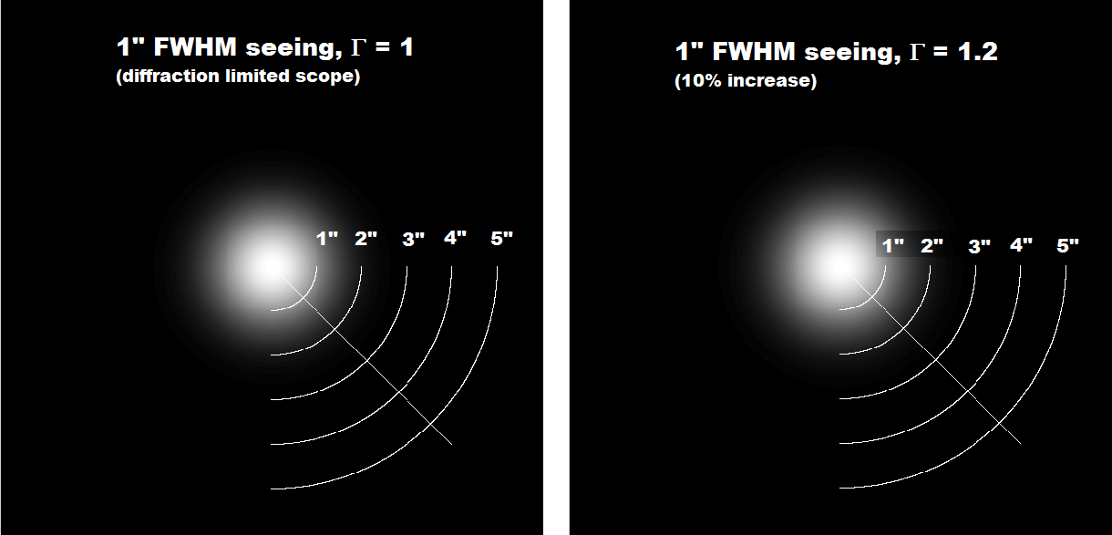
To put this in context there are below spot images (think as stars) for the above configurations.
It can be seen than the rule of 10% for the maximum spot diameter increase due to offset from the NBF provides spots with virtually no visible difference in size versus the ones limited by the diffraction and/or the scope optics.
Spots for 1″ FWHM seeing at 1x and 1.2x the diffraction limit
Spots for 1″ FWHM seeing at 1.7x and 2.2x the diffraction limit
Spots for 2″ FWHM seeing at 1x and 2.26x the diffraction limit
Conclusions
In a nutshell the tolerance (offset from the NBF distance) is tighter for good seeing and a large chip (diagonal), as we would expect.
The table below summarizes the maximum tolerances (rounded values) for a 10% spot diameter (encircled energy) increase v.s the diffraction and/or scope optical limits:
| APS-C chip | Full frame chip | |
| 1″ FWHM seeing | +/- 20 mm | +/- 20 mm* |
| 2″ FWHM seeing | +/- 50 mm | +/- 20 mm |
It should be understood that in the absence of seeing (in space) the tolerances will become much smaller, in the millimeter.
* based on 10% increase above the scope 21 mm off axis spot diameter value instead of the diffraction limit. Total spot diameter increase = 32% at the full frame chip corners. Spot diameter increase is 20% at the NBF (chip corners).
The results here are provided for guidance and information only, they are approximations related the spot diameter based to the encircled energy, large offset values would eventually lead to other aberrations, such as coma and astigmatism. Also the calculations are based to the publicly available Celestron data and documentation, which are subject to some accuracy, limitation and change.